
Electronics Metal Stampings
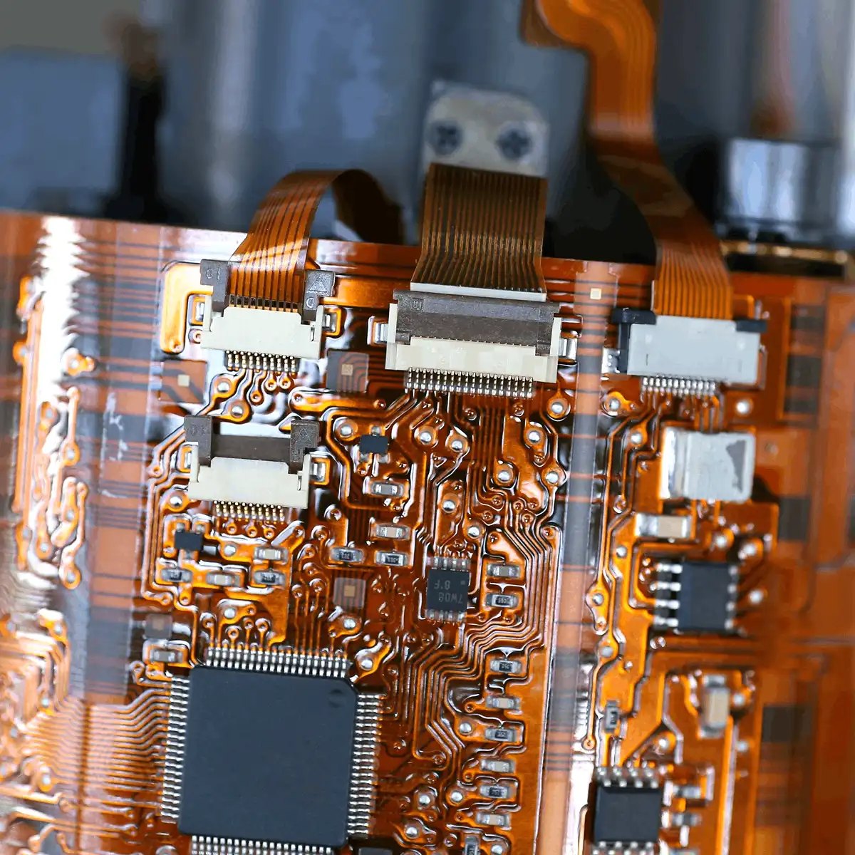
Consumer and industrial electronics require ever-smaller, ever-more-precise stamped components - from fine-pitch lead frames to board-level EMI shields.
- ISTAMPING's 0.005 mm precision enables the fine features electronics demand: lead frames, shields, connectors and press-fit pins for the world's most advanced devices.
🔒 NDA Protected⚡ 2-Hour Quote Response📁 STEP, IGES, X_T, DWG
Trusted Tier-1 & OEM Standards:
CHALLENGES WE SOLVE
Electronics Stamping Challenges & Our Solutions
ISTAMPING's 0.005 mm precision enables the fine features electronics demand: lead frames, shields, connectors and press-fit pins for the world's most advanced devices.
01
Lead frames
The Challenge
Off-spec or inconsistent lead frames cause assembly failures and field returns.
Our Solution
Fine-pitch lead frames stamped to 0.005 mm precision for IC packaging - with controlled plating and clean, burr-free edges.
02
EMI/RFI shields
The Challenge
Unreliable supply of emi/rfi shields disrupts production schedules.
Our Solution
Board-level EMI shields stamped from nickel silver, stainless steel or tin-plated steel - with solderable attachment options.
03
Connectors & pins
The Challenge
Off-spec or inconsistent connectors & pins cause assembly failures and field returns.
Our Solution
Precision stamped connectors, pins and press-fit terminals for electronic assemblies - tight tolerances for reliable insertion.
04
Sensor components
The Challenge
Unreliable supply of sensor components disrupts production schedules.
Our Solution
Miniature stamped components for sensors - housings, contacts and springs - with fine blanking tolerances for consistent performance.
Need Electronics Stampings That Meet Spec?
Send your drawing for a free DFM review and quote within 24 hours.
ENGINEERING CAPABILITIES
Electronics Stamping Specifications & Equipment
Part Specifications
| Specification Parameter | Automotive & EV Standard | High-Precision Custom |
|---|---|---|
| Part Thickness | 0.10 mm – 3.0 mm | Per drawing |
| Standard Tolerance | ±0.025 mm (±0.001 in) | Tighter on critical features |
| Positioning Precision | 0.005 mm | — |
| Press Capacity | 25–110 tons (21 presses) | — |
Equipment
Aida High-Speed Presses
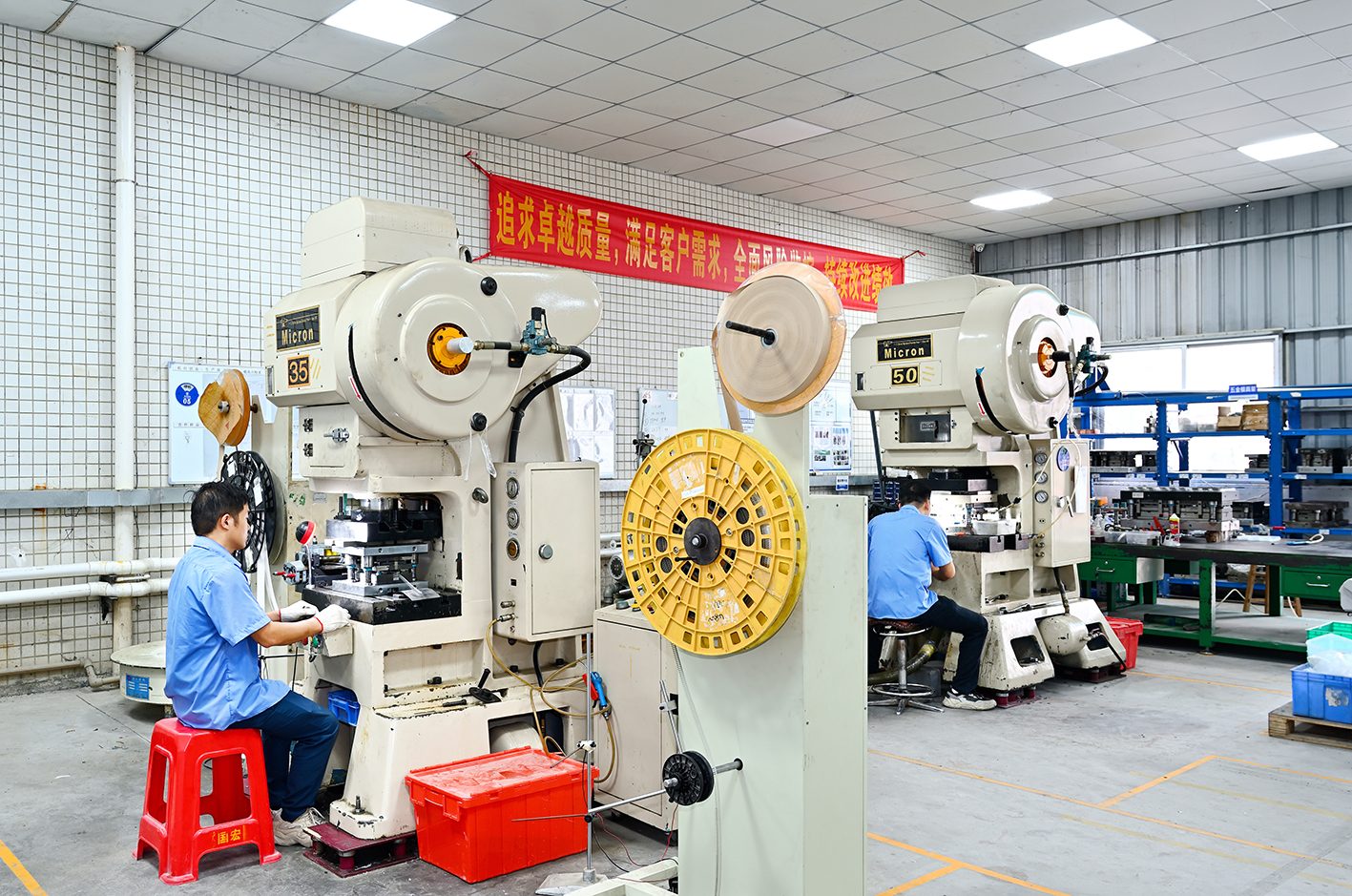
20 presses, 25–80T, up to 300 SPM with 0.005 mm positioning.
In-House Quality Lab
CMM, optical measurement and in-line vision systems verify critical features on every lot.
In-House Tool Room
Wire EDM, CNC machining and optical profile grinding keep die design and build in one loop.
Reel-to-Reel Plating
Selective gold (2-8 µm), tin and zinc (5-12 µm) plating through approved partner lines for corrosion and conductivity.
From Drawing to Production
DFM Review
Free design-for-manufacturability analysis within 24 hours.
Tooling
In-house die design, build and try-out.
Production
High-speed stamping with in-line vision inspection.
Delivery
QC, packaging and on-time shipment.
APPLICATION & INDUSTRY SOLUTIONS
Metal Stampings for Electronics
Lead frames
Fine-pitch lead frames stamped to 0.005 mm precision for IC packaging - with controlled plating and clean, burr-free edges.
EMI/RFI shields
Board-level EMI shields stamped from nickel silver, stainless steel or tin-plated steel - with solderable attachment options.
Connectors & pins
Precision stamped connectors, pins and press-fit terminals for electronic assemblies - tight tolerances for reliable insertion.
Sensor components
Miniature stamped components for sensors - housings, contacts and springs - with fine blanking tolerances for consistent performance.
Precision Stamped Components for Consumer and Industrial Electronics
Electronics require ever-smaller, ever-more-precise stamped components. ISTAMPING's 0.005 mm precision enables the fine features modern devices demand - lead frames, EMI/RFI shields, connectors and press-fit pins for IoT, smart home, wearables and telecommunications hardware.
- 0.005 mm precision for fine-pitch and miniature features
- Managed plating - selective gold, tin and nickel options
- Clean, burr-free edges for reliable downstream assembly
- High-speed production for consumer electronics volumes
Miniature Precision Stamping for Electronics
Miniature stamped parts such as lead frames, EMI shielding cans, and connector pins demand dimensional consistency measured in microns - a single out-of-tolerance feature can stall automated SMT assembly. Our stamping engineers control material springback through compensated die geometry and carefully selected alloys from 0.05 to 3.0 mm, while Aida high-speed presses running up to 300 SPM hold ±0.005 mm positioning accuracy across millions of strokes. CMM and inline vision verification keep every batch repeatable, so high-volume, high-cadence micro-stamping runs deliver the same tight tolerances from the first part to the last.
- Aida high-speed presses up to 300 SPM hold ±0.005 mm positioning accuracy for fine-pitch lead frames, shielding cans, and connector pins
- Springback-compensated progressive die design keeps thin-gauge parts (from 0.10 mm) flat and dimensionally stable across million-stroke runs
- Reel-to-reel selective plating applies conductive finishes only where required, protecting critical contact surfaces and solder joints on miniature parts
- CMM measurement plus inline vision inspection verify critical dimensions on every batch, supporting lot-to-lot consistency under IATF 16949:2016 quality management
Electronics Applications
Lead frames
Fine-pitch lead frames stamped to 0.005 mm precision for IC packaging - with controlled plating and clean, burr-free edges.
EMI/RFI shields
Board-level EMI shields stamped from nickel silver, stainless steel or tin-plated steel - with solderable attachment options.
Connectors & pins
Precision stamped connectors, pins and press-fit terminals for electronic assemblies - tight tolerances for reliable insertion.
Sensor components
Miniature stamped components for sensors - housings, contacts and springs - with fine blanking tolerances for consistent performance.
MATERIALS & COMPLIANCE
Materials for Electronics Applications
Material certifications and compliance documents available on every lot.
Brass
Common Alloys
Finishing
Copper
Common Alloys
Finishing
Phosphor Bronze
Common Alloys
Finishing
Need a Specific Alloy or Coating?
Tell us the material grade and finish — we confirm availability and certification before quoting.
🔒 MTC / CoC / RoHS available per lot
DFM & ENGINEERING SUPPORT
Design for Manufacturability for Electronics
We review material, tolerance, bend and volume economics before tooling starts.
What We Review
Lead frames geometry
Feasibility of lead frames — material formability, bend radii, tolerance stack-up and plating compatibility.
EMI/RFI shields geometry
Feasibility of emi/rfi shields — material formability, bend radii, tolerance stack-up and plating compatibility.
Connectors & pins geometry
Feasibility of connectors & pins — material formability, bend radii, tolerance stack-up and plating compatibility.
Sensor components geometry
Feasibility of sensor components — material formability, bend radii, tolerance stack-up and plating compatibility.
DFM to Production
Submit Drawing
STEP / IGES / DWG / PDF with quantity and material.
24H DFM Feedback
Cost-down suggestions and feasibility confirmation.
Tooling & Samples
In-house die build with first-article inspection.
Mass Production
High-speed stamping with SPC and PPAP documentation.
Get a Free DFM Review
Send your drawing — receive feasibility feedback and a quote within 24 hours.
STEP / IGES / X_T / DWG / PDF
QUALITY ASSURANCE & INSPECTION
IATF 16949:2016 Certified, Verified on Every Lot
CMM, optical measurement and in-line vision inspection at press speed.
 🔬 Inspection Hardware
In-House Quality Lab
- CMM & optical measurement for flat and 3D parts
- In-line vision systems inspecting at press speed
- SPC on critical features to catch drift as a trend
 🎯 Quality Standards
IATF 16949:2016 Certified
- IATF 16949:2016 automotive quality management
- ISO 14001:2015 environmental management
- PPAP documentation for automotive & EV programs
📜 TraceabilityFull Lot Traceability
- First-article inspection against the drawing
- Lot-level material traceability back to the coil
- Inspection records on every shipment
Download Sample Quality Control & Inspection Reports
Review our standard CMM inspection sheet, Material Composition Certificate, and RoHS report templates.
CASE STUDIES
Electronics Case Studies
EV Battery · Case Study
EV Busbar Case Study: Battery Pack Interconnects
High-volume busbar stamping for EV battery pack interconnects — tolerance, plating and delivery evidence.
Automotive · Case Study
Progressive Die Case Study: Automotive Terminal Program
A multi-million-piece terminal program run on progressive dies with SPC and PPAP evidence.
ORDERING PROCESS & FREQUENTLY ASKED QUESTIONS
How to Order Electronics Stampings & Frequently Asked Questions
📁 Step 1
Submit CAD & Specs
Send 2D/3D drawings (STEP, DWG, PDF) with quantity, material, and tolerance requirements.
⏱️ Step 2
24H DFM & Quotation
Our engineering team conducts DFM analysis and provides a competitive quote within 24 hours.
⚙️ Step 3
Precision Manufacturing
High-speed progressive die stamping, secondary forming, finishing, and surface treatment per your specifications.
✈️ Step 4
100% QC & Express Shipping
100% dimensional inspection, anti-corrosion packaging, and global express delivery.
What is the MOQ for Electronics metal stampings?
We support prototyping from 1 piece and mass production from roughly 100k pieces upward, depending on tooling economics.
Ready to Start Your Precision Stamping Program?
Send your drawing today for a free DFM review and detailed quotation within 24 hours.
🔒 100% Confidential | NDA Protected | 24H Response
RELATED INDUSTRIES
Related Industries

Aerospace
Aerospace metal stamping for EMI shields, connector terminals and precision brackets - material certifications, lot traceability and documented process controls on every shipment, from 25-110 ton high-speed progressive dies.
Explore Industry →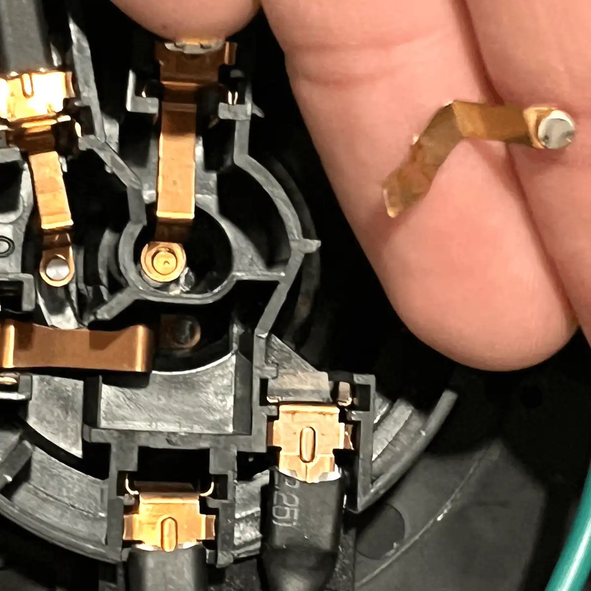
Appliance
Home appliance manufacturers require high-volume stamped components that balance cost, quality and reliability - often with complex geometries and specific finish requirements.
Explore Industry →
Automotive
The automotive industry is our most demanding and most important market. IATF 16949-certified production, PPAP documentation and zero-defect quality are the baseline for automotive stamping suppliers.
Explore Industry →