
Lead Frames
Lead frames are precision stamped metal carriers used in semiconductor packaging - providing the electrical connection path between the die and the external circuit.
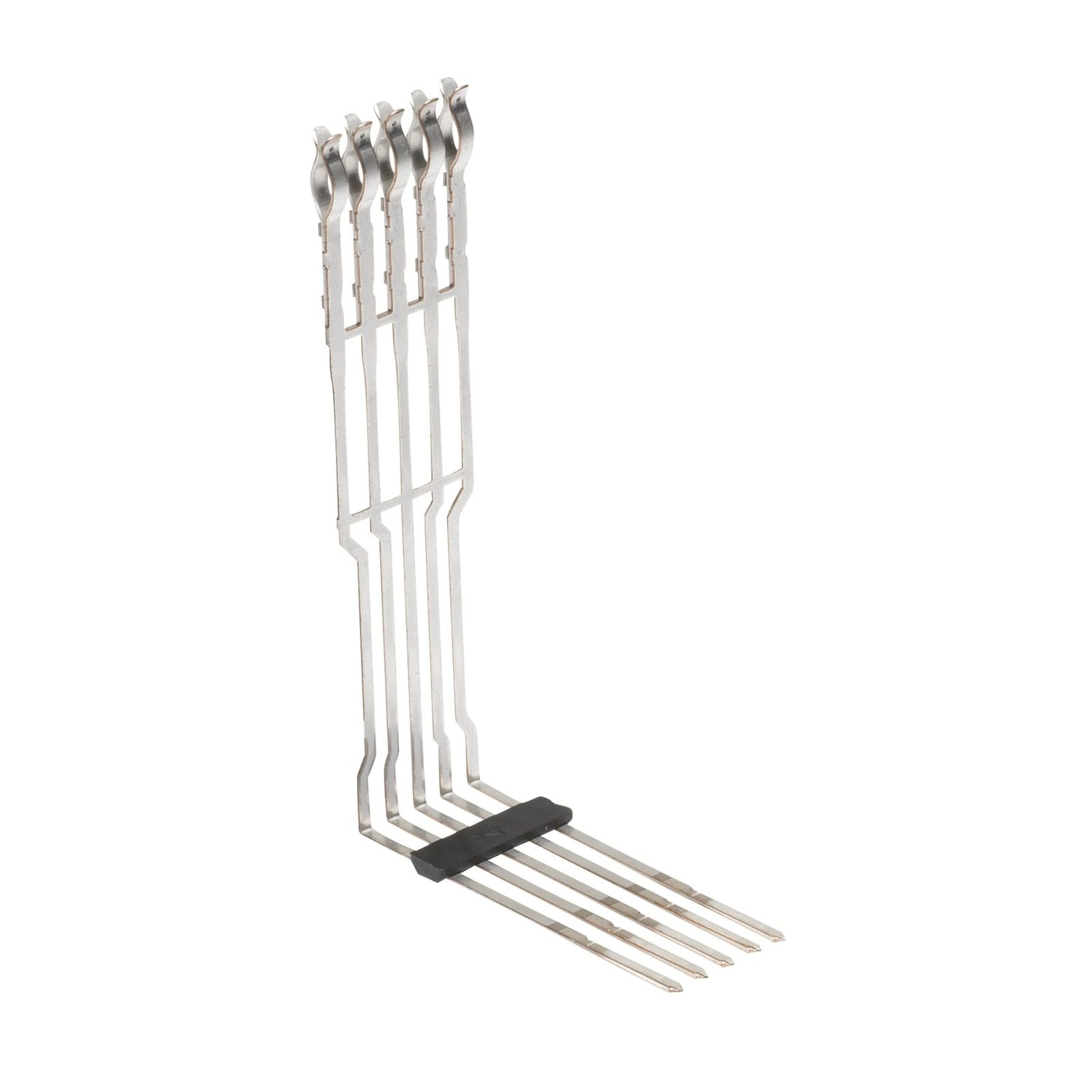
Browse the full stamped parts range for more details.
Why Lead Frames
Lead frames are precision stamped metal carriers used in semiconductor packaging - providing the electrical connection path between the die and the external circuit.
- Lead frame quality is defined by feature pitch accuracy, burr control and flatness - all critical for die-attach and wire-bonding processes. Our 0.005 mm positioning precision and managed selective plating (silver, tin) deliver lead frames that perform in the most demanding packaging environments.
- Fine-pitch leadframe features demand ultra-precision stamping, material expertise and strict flatness control.
- ISTAMPING produces ultra-precision stamped lead frames and leadframe IC components with 0.005 mm accuracy on Aida high-speed presses with automated feeding, in copper alloys, Alloy 42 and phosphor bronze - the leading frame solution for high-pin-count semiconductor packages.
FINE-PITCH PRECISION
Lead frame quality is defined by feature pitch accuracy, burr control and flatness - all critical for die-attach and wire-bonding processes. Our 0.005 mm positioning precision and managed selective plating (silver, tin) deliver lead frames that perform in the most demanding packaging environments.
Types of Lead Frames We Produce
Technical Specifications
Material thickness
0.10 – 0.50 mm
Positioning precision
±0.005 mm
Pitch / feature
Fine-pitch down to 0.4 mm
Press capacity
25 – 80 tons (high-speed)
Production speed
Up to 300 SPM
Plating
Selective silver / tin / nickel
Common Materials
- C194 / C7025 High-Performance Copper
- C5191 Phosphor Bronze
- Alloy 42 (Fe-Ni)
- C1100 Copper
How We Manufacture Lead Frames
IC Package Role
A lead frame is the metal carrier that provides the electrical path between the semiconductor die and the external circuit, and a mechanical skeleton for molding. We engineer frames for wire-bond and clip-bond packages.
Stamping vs Etching
For high-volume, thin, high-conductivity frames we use high-speed progressive stamping - higher throughput and lower unit cost than chemical etching, with superior edge quality and dimensional repeatability.
Fine-Pitch Progressive Tooling
Precision progressive dies built 100% in-house form leads and tie bars at ±0.005 mm, holding fine pitch down to 0.4 mm across long runs.
High-Speed Stamping
Lead frames are stamped on Aida high-speed presses with automated feeding and in-process monitoring, up to 300 SPM with burr-free edges.
Selective Plating
Reel-to-reel selective silver or tin plating is applied only on bonding and soldering areas, controlling cost while meeting electrical and reliability specs.
Flatness and Tie-Bar Design
Die-attach and wire-bonding tolerate almost no out-of-flat variation, so tie-bar geometry, carrier rail design and stress release during blanking are engineered together. Frames ship on tape or lay-flat with crossection and camber verified per lot.
Cleanroom Inspection
Dimensional and visual inspection under IATF 16949:2016 - including cleanroom handling for sensitive packages - verifies flatness and burr control before shipment.
Design-for-Manufacturability Support
Our engineers review your lead frame at the quoting stage - pad geometry, pitch, material grade and plating zones - and recommend design-for-manufacturability changes that improve yield and lower tooling cost. Existing dies can be taken over and optimized for our high-speed presses. For the process decision itself, see our <a href="/news/lead-frame-etching-vs-stamping/">lead frame etching vs stamping comparison</a>, the <a href="/news/lead-frame-surface-mount-guide/">surface-mount lead frame guide</a> and the <a href="/news/lead-frame-stamping-tolerances-alloys-process/">tolerance & alloy selection guide</a>.
FAQ
Questions Buyers Ask
What is a lead frame used for?
A lead frame carries the electrical connection between the IC die and the external circuit, and provides the mechanical structure for packaging. We produce frames for wire-bond and clip-bond semiconductor packages.
Stamping or etching for lead frames?
For high-volume thin, high-conductivity frames, high-speed stamping offers higher throughput, lower unit cost and better edge quality than chemical etching - our standard approach.
What materials and pitch can you hold?
We stamp C194/C7025 copper alloys, phosphor bronze and Alloy 42 at ±0.005 mm precision, with fine pitch down to 0.4 mm standard and 0.25 mm lead pitch program-dependent.
How are lead frames packaged for the assembly line?
Frames ship on tape or lay-flat per your die-attach equipment, with flatness (camber and crossection) verified per lot and cleanroom handling for sensitive packages.
Which is cheaper for high volume: stamped or etched lead frames?
Above roughly tens of thousands of units, progressive stamping wins on throughput and cost per pin, and it holds tighter flatness on copper alloys; etching stays the right call for complex 2.5-D geometries and very low volumes. Our comparison guide breaks down the crossover point.
Recommended Products
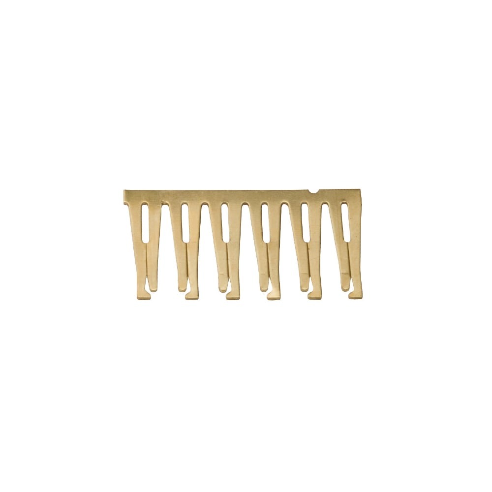
Terminals
Terminals are necessary to connect various circuits or systems. Sometimes called electrical connectors, these components are used to transfer electrical current from a power or grounding source to an electrical system.
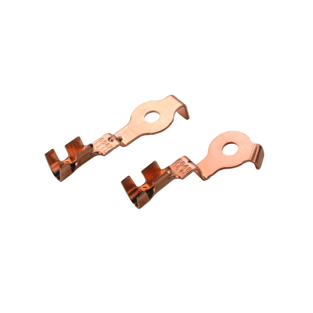
Wire & Cable Connectors
Wire and cable connectors, also known as crimp terminals, crimp wire connectors, crimp cable connectors and eyelet terminals serve a simple but essential purpose of connecting electrical wires and cables to other parts and modules within the entire electrical system of vehicles, appliances, control systems and other electrical applications.
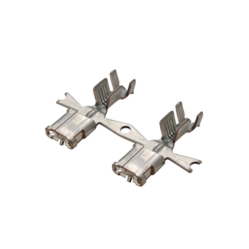
Assemblies
Assemblies are complete finished products or sub-assemblies built from multiple stamped components joined together - often combining metal stampings with plastic parts, hardware and inserts.