
Telecommunications Metal Stampings — Tolerance Under RF Load
Telecommunications infrastructure demands stamped components that perform reliably outdoors for decades - connectors, shielding and mounting hardware for networks that never sleep.
NDA ProtectedFast Quote ResponseSTEP, IGES, X_T, DWG

Trusted Tier-1 & OEM Standards:
CHALLENGES WE SOLVE
Telecommunications Stamping Challenges & Our Solutions
Four recurring telecommunications failure modes seen in incoming RFQs — and how each is prevented on our line.
01
Telecom connectors
The Challenge
Contact-resistance drift from tolerance creep on terminal features causes intermittent failures in the field.
Our Solution
Held with 100% critical-dimension checks at press speed and plating-thickness verification per lot.
02
EMI shielding
The Challenge
Incomplete shield form recovery breaks grounding continuity and lets EMI escape spec.
Our Solution
Form recovery and ground-contact faces verified by CMM first article plus in-line vision.
03
Base station hardware
The Challenge
Hole-position and flatness drift on mounting parts forces assembly rework at the OEM line.
Our Solution
Die correction at build plus SPC on hole position and flatness keeps fixtures mating first time.
04
Fiber optic components
The Challenge
Tolerance stack-up across progressive stages drifts critical features out of spec lot by lot.
Our Solution
Held with 0.005 mm positioning precision and 100% dimensional inspection before packing.
Need Telecommunications Stampings That Meet Spec?
Send your drawing — engineering runs a free DFM review and pricing follows the review.
ENGINEERING CAPABILITIES
Telecommunications Stamping Specifications & Equipment
Part Specifications
| Specification Parameter | Automotive & EV Standard | High-Precision Custom |
|---|---|---|
| Part Thickness | 0.10 mm – 3.0 mm | Per drawing |
| Standard Tolerance | ±0.025 mm (±0.001 in) | Tighter on critical features |
| Positioning Precision | 0.005 mm | — |
| Press Capacity | 25–110 tons (21 presses) | — |
Equipment
Stamping Presses
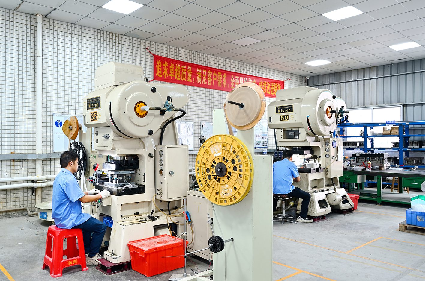
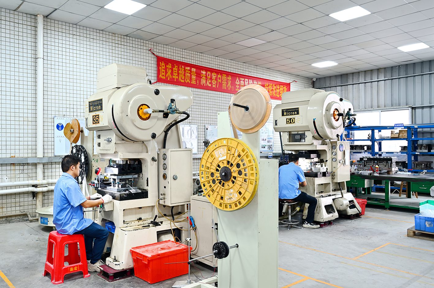
21 presses, 25–110T — up to 300 SPM with 0.005 mm positioning on the high-speed line.
In-House Quality Lab
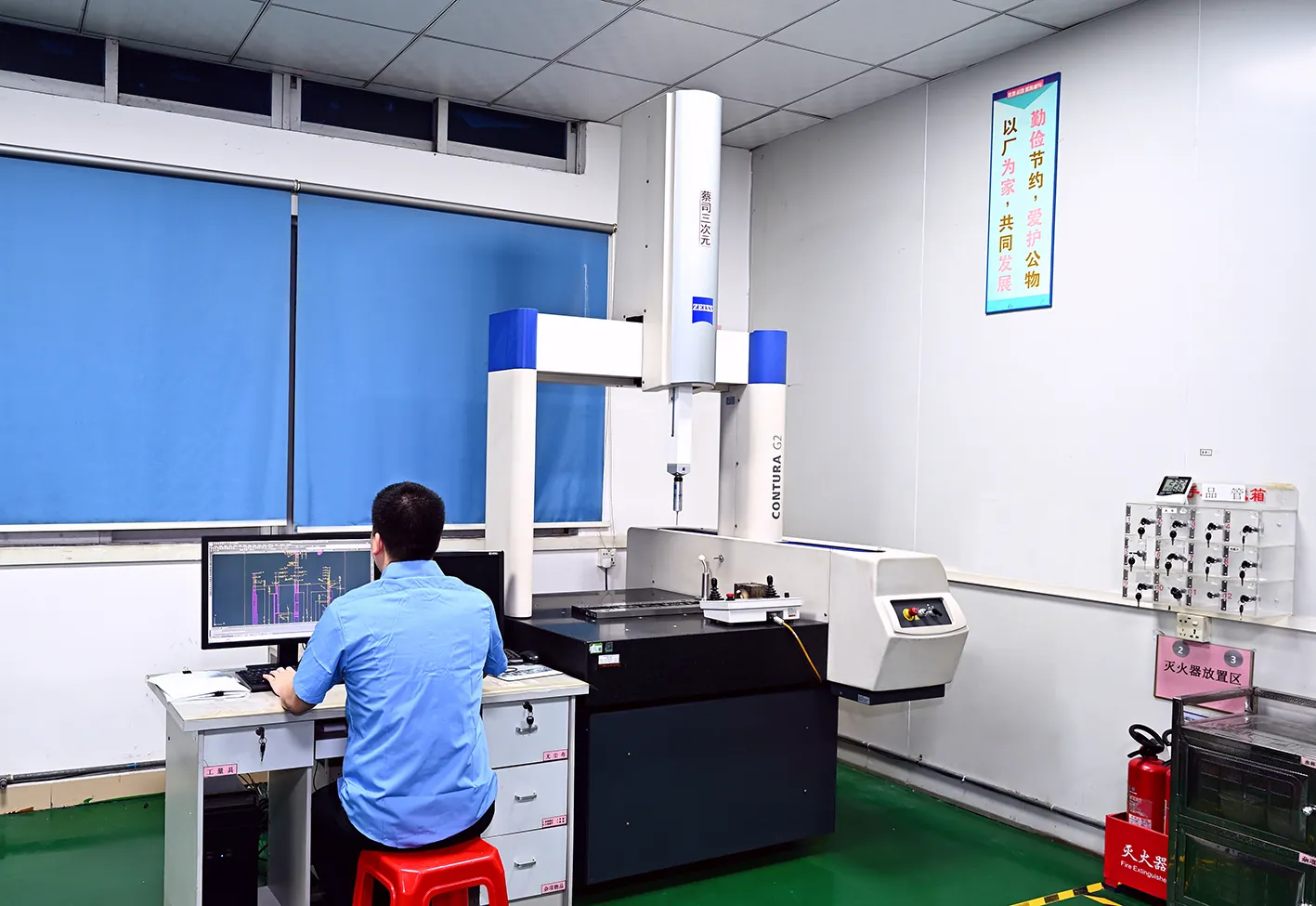
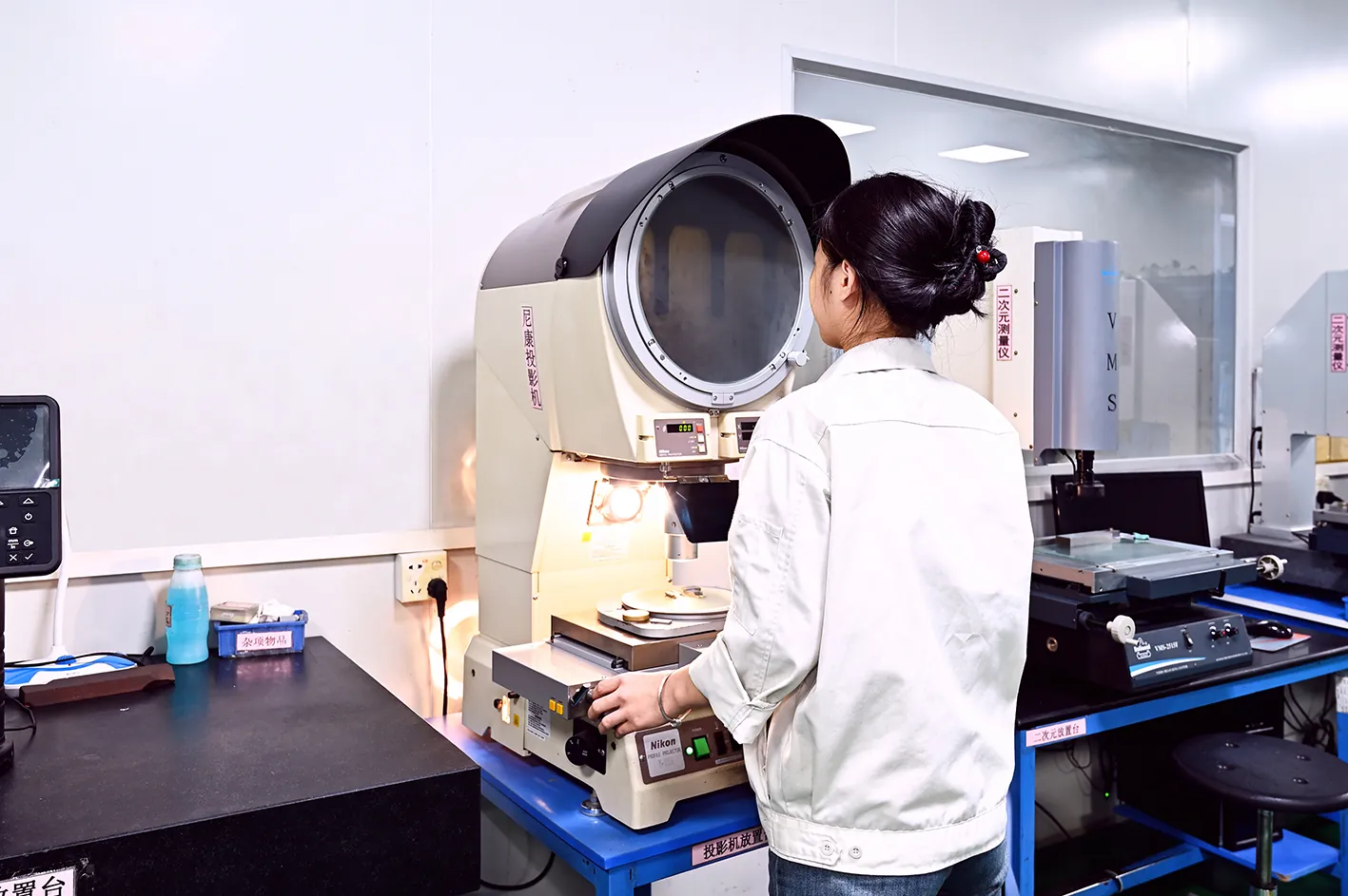
CMM and optical measurement verify critical features on every lot.
In-House Tool Room
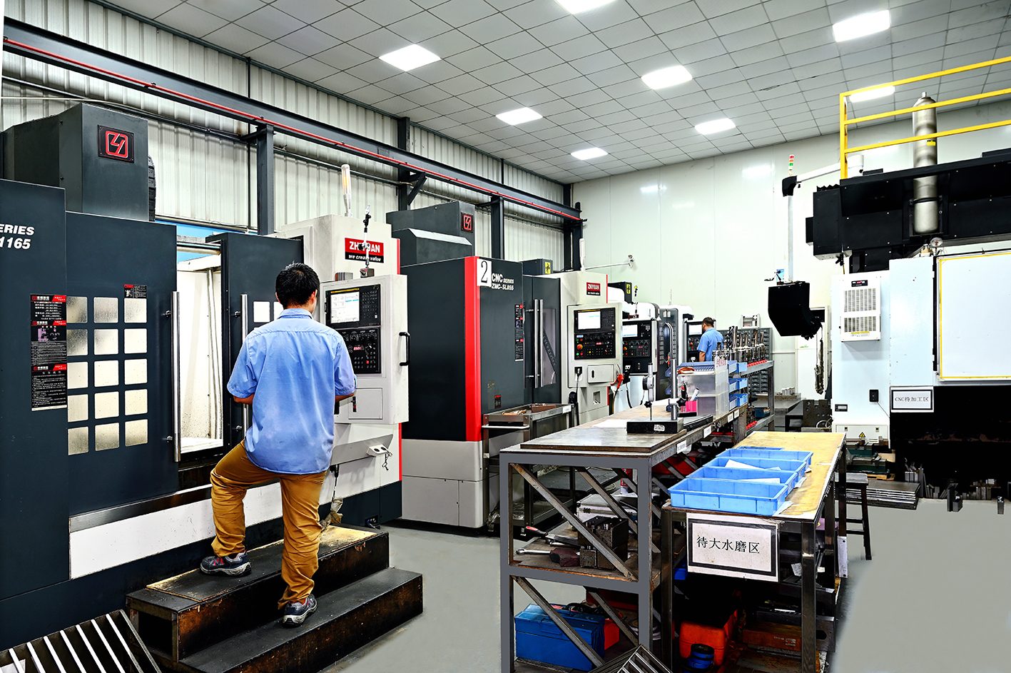
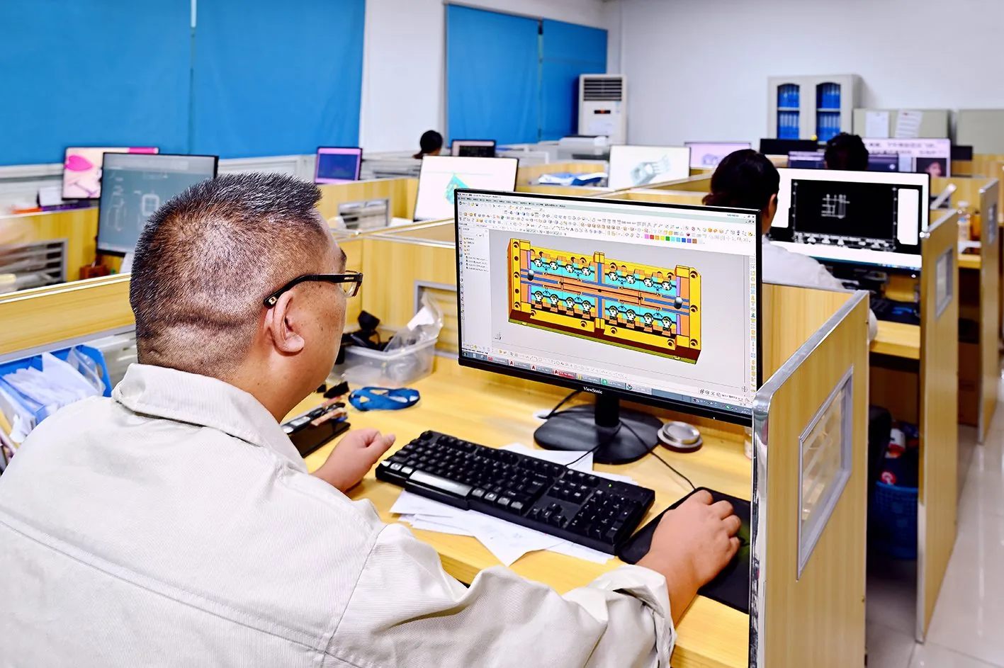
Wire EDM, CNC machining and optical profile grinding keep die design and build in one loop.
Reel-to-Reel Plating
Selective gold (2-8 µm), tin and zinc (5-12 µm) plating through approved partner lines for corrosion and conductivity.
APPLICATION & INDUSTRY SOLUTIONS
Metal Stampings for Telecommunications
Telecom connectors
Stamped connector terminals for telecom infrastructure - reliable electrical contact with plating for outdoor longevity.
EMI shielding
EMI shielding stamped for base stations and network equipment - protecting sensitive electronics in demanding environments.
Base station hardware
Stamped brackets, clips and mounting hardware for base stations - durable materials built for outdoor service.
Fiber optic components
Precision stamped components for fiber optic systems - alignment parts and brackets with tight tolerances.
Telecommunications stamping
Telecommunications Metal & Part Stamping
Telecom hardware we stamp: connector terminals and crimp pins, EMI shield cans for baseband and switching units, antenna mounting brackets and clamps, and fiber-alignment frames. Rooftop and tower exposure decides the spec, so finishes are selected per site class — nickel or tin over copper alloys for contact surfaces, zinc flake and passivation on brackets — and shielding contact geometry is held on ±0.005 mm presses so shield cans mate against gasket fingers without gaps.
- Plating and coatings engineered for decades of outdoor service
- Reliable electrical contact for networks that never sleep
- High-volume production for telecom infrastructure demand
- Precision tolerances for base station and network hardware
Telecommunications stamping
RF-Ready Stamping for Telecom Infrastructure
Telecom infrastructure lives or dies on signal integrity, and the stamped parts inside it must hold tolerance under RF loads that expose even the smallest deviation. Connector shells, EMI shielding cans, and base station hardware have to maintain continuous shielding contact across thousands of mating cycles while surviving years of rooftop and tower exposure to UV, salt spray, and thermal cycling. Our IATF 16949:2016 certified press shop delivers these small precision stampings with ±0.005 mm positioning accuracy on high-speed presses up to 300 SPM, in material thicknesses from 0.05 to 3.0 mm, so RF assemblies get repeatable geometry part after part.
- ±0.005 mm positioning accuracy on high-speed presses up to 300 SPM keeps RF-critical connector and shield geometry consistent across full production runs
- Reel-to-reel selective plating deposits shielding-grade finishes exactly where contacts and grounding points need them, cutting cost without breaking EMI continuity
- CMM inspection plus inline machine vision verifies shielding contact surfaces and mating dimensions on every batch before parts leave the floor
- In-house tool design and build supports fast DFM iteration on connectors, EMI shields, and base station hardware, with fast DFM feedback on new designs
INSIDE THE PLANT
Inside Our Telecommunications Stamping Line
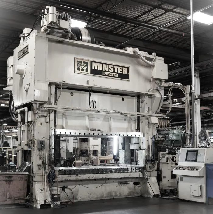
Real equipment and inspection floor from our Dongguan plant — 25–110T high-speed presses, in-house tool room, and a CMM lab running first-article inspection on every program.
MATERIALS & COMPLIANCE
Materials for Telecommunications Applications
Material certifications and compliance documents available on every lot.
Brass
Common Alloys
Finishing
Copper
Common Alloys
Finishing
Phosphor Bronze
Common Alloys
Finishing
Stamping on Your Alloy or Coating?
Send the grade, gauge and part drawing — we confirm stampability, die and feed design, and quote on 25–110T presses at ±0.005 mm.
MTC / CoC / RoHS available per lot
DFM & ENGINEERING SUPPORT
Design for Manufacturability for Telecommunications
We review material, tolerance, bend and volume economics before tooling starts.
What We Review
Telecom connectors geometry
Contact geometry — mating tolerance, plating thickness for conductivity, and reel-feed orientation for in-line inspection.
EMI shielding geometry
Shield enclosure — form recovery after forming, ground-contact faces, and aperture tolerance over the protected circuit.
Base station hardware geometry
Mounting features — hole position and flatness under vibration, bend-radius margins on thin gauge.
Fiber optic components geometry
Feature walk-through — material formability, bend radii, tolerance stack-up and plating compatibility for this part.
What Our DFM Review Checks
Bend radii
Inside radius held at R≥1.0t on spring tempers; tighter bends flagged for anneal or grade change before die design starts.
Holes & cutouts
Hole diameter ≥0.8t, pushed to 0.6t only with hardened punch steel; thin-gauge cutouts checked for tear-out.
Burr & edge quality
Burr height held under 0.05 mm so parts mate flat in assembly and plating adheres at the edges.
Tolerance & plating impact
Critical features piloted to ±0.005 mm; plating thickness (gold 2-8 µm, tin/zinc 5-12 µm) compensated in die design.
Get a Free DFM Review
Send your drawing — receive engineering feasibility feedback, with pricing to follow.
STEP / IGES / X_T / DWG / PDF
QUALITY ASSURANCE & INSPECTION
IATF 16949:2016 Certified, Verified on Every Lot
CMM, optical measurement and 100% dimensional inspection at press speed.
 Inspection Hardware
In-House Quality Lab
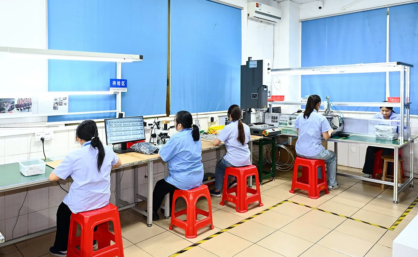
- CMM & optical measurement for flat and 3D parts
- In-line vision systems inspecting at press speed
- SPC on critical features to catch drift as a trend
 Quality Standards
IATF 16949:2016 Certified
- IATF 16949:2016 automotive quality management
- ISO 14001:2015 environmental management
- PPAP documentation for automotive & EV programs
 Traceability
Full Lot Traceability
- First-article inspection against the drawing
- Lot-level material traceability back to the coil
- Inspection records on every shipment
Talk to Our Engineers About Quality Documentation
Tell us what your project requires, and our team confirms which inspection and material documentation can be included with your quote.
In-House Tool Room
Made in Our Own Tool Room
Every progressive die behind our stamped parts is 100% in-house stamping tooling — design, machining, assembly and T1 trial all under our roof. That is why tooling issues get solved on the shop floor in hours, not by email exchange with an outside die shop.
±0.001 mm Achieved
Combined machining accuracy down to ±0.001 mm, Ra0.05 µm surfaces and Ø0.05 mm micro end mills for tight die features.
30 In-House Machines
30 die-making machines — wire EDM, CNC and precision grinding — keep every die build and repair on our own schedule.
2–5 Weeks for Stamp Dies
Typical stamping die delivery in 2–5 weeks, with T1 trials run on our own presses before you commit to volume.
One Accountable Chain
Self-designed progressive dies, machined in-house, run at 60–300 SPM with CCD inline inspection — no outsourced-die handoff where quality falls between suppliers.
CASE STUDIES
Telecommunications Case Studies
Aug 28 · 7 min read
EV Busbar Case Study: Battery Pack Interconnects
High-volume busbar stamping for EV battery pack interconnects — tolerance, plating and delivery evidence.

Aug 28 · 7 min read
Progressive Die Case Study: Automotive Terminal Program
A multi-million-piece terminal program run on progressive dies with SPC and PPAP evidence.
Oct 20 · 1 min read
Copper Busbars for Energy-Storage Cabinets, Progressive-Die Formed
A manufacturer of energy-storage and EV-charging cabinets came to us with a busbar problem: parts were cut and formed one operation at a time, so…
ORDERING & FAQ
How to Order Telecommunications Stampings & Frequently Asked Questions
From drawing to delivered parts: a four-step path with engineering review at the front and 100% dimensional inspection at the back — then the questions buyers ask us most.
Step 1
Submit CAD & Specs
Send 2D/3D drawings (STEP, DWG, PDF) with quantity, material, and tolerance requirements.
Step 2
DFM Feedback & Quotation
Our engineering team conducts DFM analysis and follows up with a competitive quote after the review.
Step 3
Precision Manufacturing
High-speed progressive die stamping, secondary forming, finishing, and surface treatment per your specifications.
Step 4
100% QC & Express Shipping
100% dimensional inspection, anti-corrosion packaging, and global express delivery.
What is the MOQ for Telecommunications metal stampings?
We support prototyping from 1 piece and mass production from roughly 100k pieces upward, depending on tooling economics.
How do you guarantee material authenticity and quality documentation?
Every batch comes with material certificates and inspection reports. Heat treatment and plating logs are provided upon request.
What packaging and anti-corrosion protection do you apply for international shipping?
All finished telecommunications metal stampings undergo ultrasonic cleaning, anti-rust treatment, individual protective sealing, and padded shockproof box packaging.
Can you stamp non-standard custom shapes or complex geometries?
Yes! We specialize in complex telecommunications metal stampings including deep-drawn forms, multi-bend geometries, micro features, and tight-tolerance profiles per CAD specs.
Ready to Start Your Precision Stamping Program?
Send your drawing today — engineering runs a free DFM review and detailed pricing follows the review.
100% Confidential | NDA Protected | 24H Response
WHERE TO NEXT
See What Else We Stamp
Same ±0.005 mm discipline, different parts. Pick the market closest to yours and see what we run there.
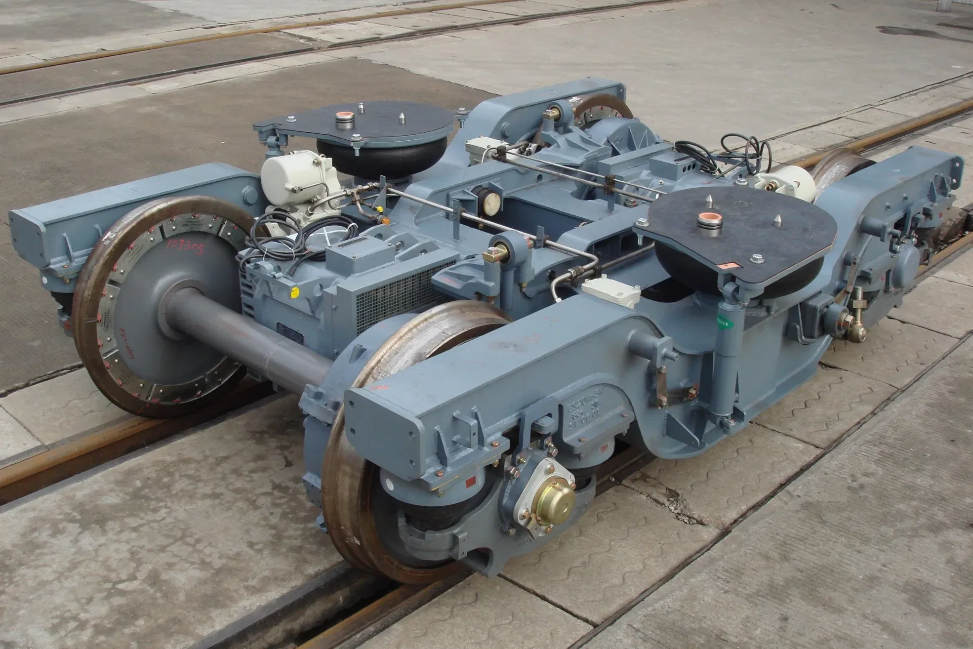
Rail & Transit
Spec hardware that shrugs off decades of vibration, humidity and washdown without service.
Explore Industry
Aerospace
Stamp shields, terminals and brackets on mill-certified coils with lot records.
Explore Industry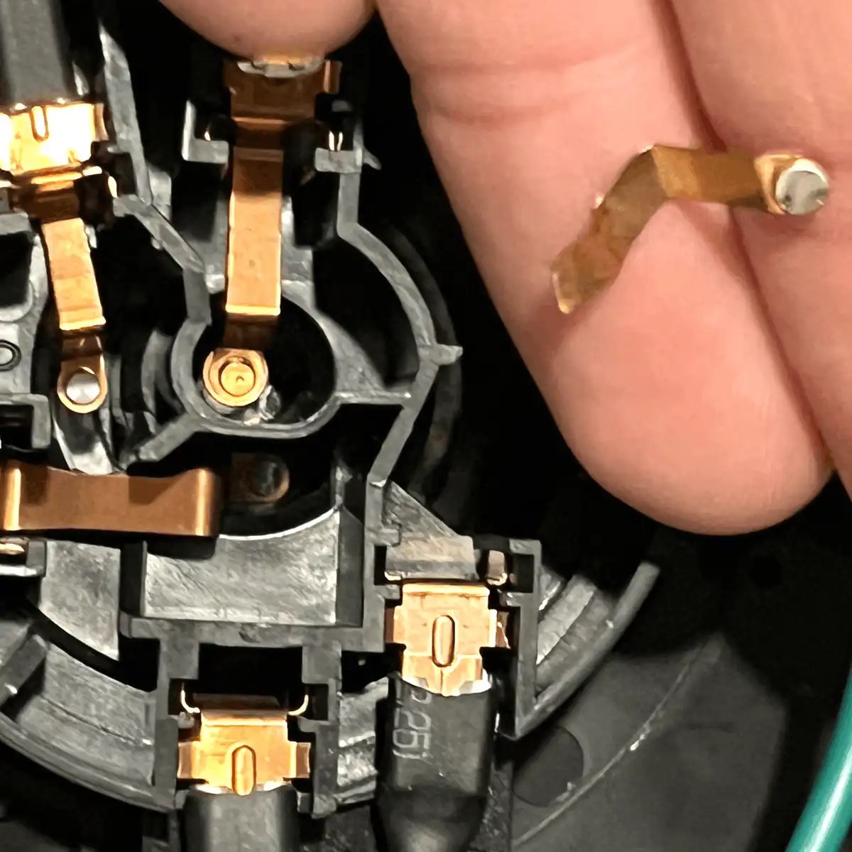
Appliance
Bring per-piece cost down with reel-fed progressive-die runs at up to 300 SPM.
Explore Industry